Turbidity sensor internal electronics: Building a first prototype (Part 1 – drawings, components, breadboard, and soldering)
So this blog post is coming a full year after I started researching, designing, and building this turbidity sensor. For the sake of “organization,” I decided to dedicate this first part to the internal electronics of the turbidity sensor prototype. Part 2 will be dedicated to the actual sensing “head” and the waterproof housing (since it’ll all be one piece) (Addendum 31-01-2022: you can find part 2 here). If you’re curious to know how this project started, you can read about it here.
Internal electronic components and breadboard assembly
The first version of the sensor was obviously built on a breadboard, so I could figure out how to program the thing and make sure everything is working properly. (I once tried to build an entire system from scratch and soldering all of the components immediately… it didn’t go so well. You can watch a video here of 24-year-old Jess doing her best at the time.) Anyways, the point is to always test everything on a breadboard.

From the picture above you can see all of the components I have broken up into two categories:
Actual turbidity sensing components:
- 850nm IR led
- 2x light-frequency converters
- 2x 10uF decoupling capacitors
- 3x plano-convex plastic molded lenses
- 3D printed housing
Everything else to make a functional turbidity sensor (this post is dedicated to these components and their assembly):
- ESP32-DevKitC-32D
- Micro SD card reader
- Micro SD card
- 9V battery
- 9V battery snap connector
- Slide switch
- 3x logic-level P-Channel MOSFETS
- 2x logic-level N-Channel MOSFETS
- A bunch of resistors
- Prototyping board
Below you can see my first-time-ever hand-draw schematics of the system:

Soldering the turbidity sensor internal electronics onto a prototyping board
Once the turbidity sensor internal electronics were working on the breadboard, I figured it was time to solder everything together onto a prototyping board and shove it into some sort of waterproof PVC-inspired housing (oh! and build 5 more duplicates for our next experiments….).
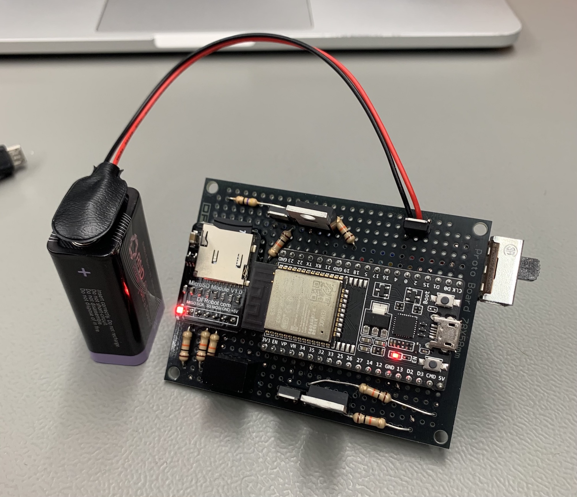
In the pictures below you can see what the soldered versions of the sensor look like. With the first prototype/solder-job, I put the MOSFETS on the “wrong” side of the board. I say wrong because I quickly realized it was much easier to flip them to the opposite side of the board, where I then had better access to soldering the boards.
Even more problems
After I finished soldering the first board, I saw something fishy. Basically, my 9V battery was directly connected to the 5V pin. If you look at my schematics above, you’ll see I have a DC/DC converter in my Power Supply schematic (I added the converter in the schematic AFTER I found this problem…). The DC/DC converter wasn’t originally in my breadboard design, and everything seemed to work fine (except my SD card reader would sometimes get angry and stop working entirely, but I assumed it was because the SD card reader just hated me). But once I started soldering, I realized I couldn’t directly shove 9V into the 5V pin (actually, this ESP32-DevKitC-32D has an onboard converter that takes max 16V (I think) into the 5V pin and steps it down to 3.3V – so everything connected to the board would work fine, but my SD card Vin is connected directly to the 5V pin and not a 3.3V pin. So my SD card Vin and my detectors Vin (which both take 5V max), were actually receiving 9V – no bueno).

So I ordered a DC/DC converter (this one) and added it to my prototyping board. After I finished soldering everything, I checked my connections with a voltmeter. I found some bad joints and fixed them.
Turbidity sensor internal electronics final test
Finally, the worst part was approaching… I had to actually test my boards:S Maybe you’re thinking “But Jess, shouldn’t you have tested your boards before making 6 of them?” And to answer your question, yes! You’re right! The only reason I didn’t make 1 board and test it before making 6 duplicates is because I was waiting for the DC/DC converters to arrive. So I figured I might as well solder as much as I can before the final components arrive. Anyways, what I found in my tests is that nothing worked:D But upon further investigation, it looks like my DFRobot prototyping board has two rails that are connected and meant to be used as VCC and GND rails. In my opinion, this is very bad engineering design because the rails don’t look any different than the non-connected rails. A quick fix was to just make some cuts along the rails to break those connections. You can see the cuts in the image below.

After making those cuts, the sensor worked! You can see the finished turbidity sensor internal electronics in the photo below. Next step is to build a waterproof housing:)
(Comments coming soon! I’m still trying to figure out WordPress:D For now, please email me. And I can make an addendum to the post.)
Addendum 29-04-2021:
I figured out how to add comments!
Addendum 03-05-2021:
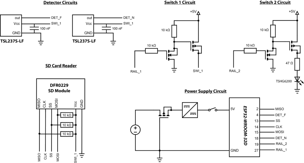
Here are some “proper” schematics:
Addendum 23-12-2021:
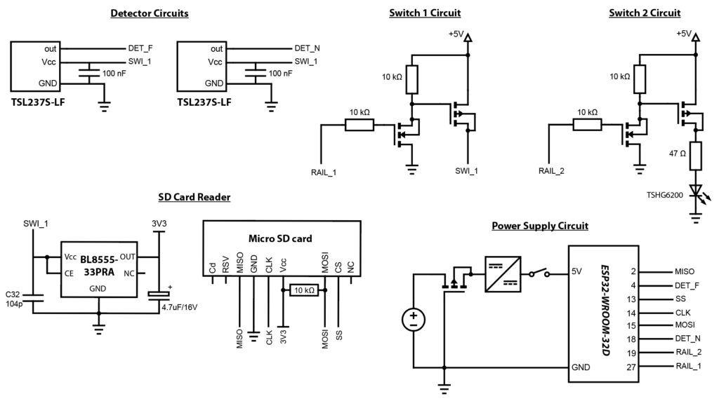
I have two pieces of information to share with you today. 1) I’m going to go through each of these subcircuits on the schematic and explain them properly and 2) I actually found a mistake in my schematic and will explain the correction. Here’s the new schematic (everything is the same except the SD card reader circuit):
Subcircuit explanation
The sensor has five sub-circuits. I connected a 9V battery to the Power Supply Circuit, which supplies power to the entire system. And I used a P-channel MOSFET here to prevent any damage to the ESP32 microchip in case the battery is accidentally connected backwards. As described earlier in the post, I also used a DC-DC converter to step down the battery voltage from 9V to the ESP32-WROOM-32D input voltage of 5V and I installed a slide switch between this converter and the 5V line to turn the sensor on and off.
You can control both switch circuits from pins on the ESP32-WROOM-32D module by setting the pins from high (3.3V) to low (0V). Both circuits have an N- and P-channel MOSFET combination which are used to supply or cut the current flowing from +5V. Switch 1 Circuit is used to turn off and on all of the electronic components (detectors, SD card reader) between readings to save power. By setting pin 27 on the ESP32-WROOM-32D to high and low in the code for Switch 1 Circuit, current would either flow from 5V to SWI_1 (high) or no current would flow (low). When current flows, everything connected to SWI_1 is supplied with power. I use the same principle for Switch 2 Circuit; when pin 19 on the ESP32-WROOM-32D is set to high, current flows from +5V to ground and supplies power to the TSHG6200 LED. When pin 19 is low, the LED is off.
I programmed the ESP to take a measurement every minute and between readings, to enter deep sleep. When the ESP is taking a measurement, it will set pin 27 to high and supply power to the SD Card Reader and the Detector Circuits. At the same time, it will take a frequency reading first with pin 19 set to low (LED off) and then again with pin 19 set to high (LED on), for the off-on differencing measurement. Once the differencing measurement is finished, the ESP will turn pin 27 low which should cut all power to the detectors and the SD card reader, then the ESP will enter deep-sleep until it is time to take another measurement.
SD card reader correction
The SD card reader we used in our experiments was the DFRobot MicroSD module (DFR0229). But this module should only be used with a board sitting at 5V (e.g. Arduino UNO), but our ESP development board sits at 3.3V (this is probably why the SD card reader was always angry with me!). For the sake of our experiments, we quickly corrected this error by removing the voltage divider on the DFR0229 (see datasheet) and connecting a 10K resistor to pull up the MOSI line. The SD Card Reader schematic above is the final schematic after our adjustments. In the future, I would suggest that you use a 3.3V microSD card reader like the Adafruit MicroSD breakout.
Please leave me a comment!:)
I guess you’ve seen this project.
https://thecavepearlproject.org/
Hi! Yes, The Cave Pearl project has been super helpful to me as I was learning to make my own sensor:)
If you don’t mind me asking, why are some of the components crossed out? Thanks!
I have a plugin on the website that checks broken links and for some reason it thinks this link is broken and I’m not sure how to fix it:S